Toward Self-Powered Medical Implants
Roger Shih


| [ Introduction ] | [ Principle ] | [ Device Design ] |
Piezoelectric Semiconducting Nanowires
Introduction:
Dr. Zhong Lin Wang has extensively explored the potential of piezoelectric semiconductor nanowires as a power source for tiny implantable devices.
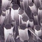
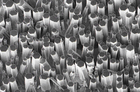
Zinc oxide (ZnO) nanowires are fabricated by depositing gold nanoparticles as catalysts on a substrate, then heating them with ZnO powder in a tube furnace while argon gas is flowed through as a carrier. The result is a mat of hexagonal ZnO columns between 1-3 μm in height and 30-100 nm in diameter, each capable of generating a few mV of potential and minute amounts of current on flexion. Additional modifications may be made to improve the structural properties, such as adding a layer of polymer around the base of the wires to strengthen their adhesion to the substrate.
Principle:
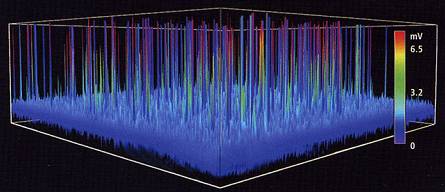
Zinc oxide is unique in having both piezoelectric and semiconducting properties. The former enables voltage generation by deforming the material’s structure and disturbing its normally-uniform charge distribution. The latter, meanwhile, enables controlled storage and release of the induced piezoelectric charge.
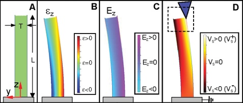
Below you can see the modeling of the piezoelectric effect in a ZnO nanowire, including the longitudinal strain in the structure as it bends (B), the induced longitudinal electric field (C), and the resulting potential distribution, with positive charge on the stretched side and negative charge on the compressed side.
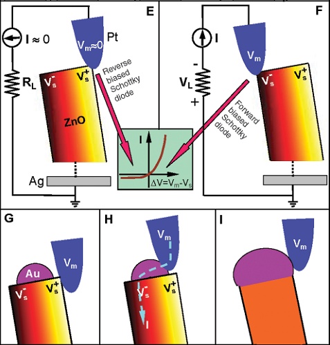
The semiconducting effect is illustrated in a related set of figures below. The interface between the ZnO wire and the platinum (Pt) electrode was found to be a Schottky barrier, constituting a diode or switch that insulates the stretched side of the wire (E) and only allows current flow when the electrode contacts the compressed, negatively-charged side (F). In cases where a particle of gold (Au) catalyst remains on the tip of the wire, its size affects the conductive behavior: If it is smaller than the wire diameter, the electrode remains insulated while touching the stretched side of the wire (G). Once the electrode touches the gold tip, however, a circuit to the conductive compressed side is formed that allows current to pass through (H). In addition, if the gold particle is larger than the wire diameter, the electrode will have difficulty pushing the side of the wire without touching the tip and closing the circuit, leading to current leakage (I).
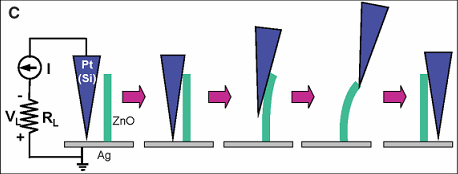
Thus the basic functional unit for a current-generating device is a semiconducting piezoelectric nanowire and an electrode, which interact as follows: External force pushes the electrode against the side of the wire, flexing it and producing piezoelectric charge which is stored thanks to the semiconductor’s insulating properties on the stretched side. As the electrode continues bending the wire and storing charge, it slips up the wire’s length until it scrapes over the tip and contacts the compressed side, at which point a circuit is formed and the stored piezoelectric charge is released as current. The electrode then finishes passing over the wire and drops down the other side, allowing the latter to spring back into a straight position, ready for a second pass in the reverse direction. Moving the electrode back and forth over the wire thus produces a pulse of current.
Device Design:
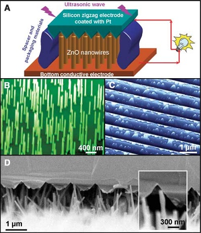
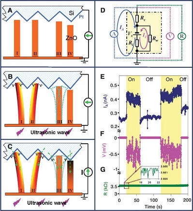
Once Dr. Wang established the basic mechanism of current production, he began exploring designs that could flex many wires in parallel to obtain more power. In 2007, he published a design which employed a zigzagged electrode to flex an entire forest of nanowires at once. Rather than moving laterally, however, the electrode is pushed down on the wires by ultrasonic waves or hydraulic force, such as might be produced in blood in the body by a beating heart or contracting blood vessels. The resulting electrode movement either compresses the wires vertically and generates current, or wedges them apart and produces current when the tips touch the sides of adjacent wedges. In this way a current of less than 1 nA was drawn from a 2 mm² substrate, but Dr. Wang estimates that this can be improved by two to three orders of magnitude with design optimizations, such as better control of the electrode-wire spacing and alignment, and more uniform wire height so that more can be effectively activated with each stroke.
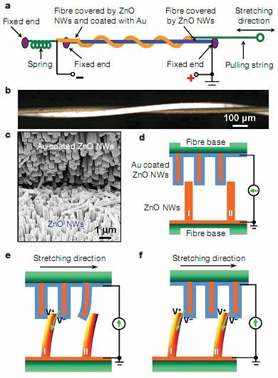
An alternative design in 2008 aimed to harvest lower-frequency movement by fabricating the wires and electrodes on textile fibers, which could then be drawn against each other to produce electricity. The electrodes in this design were themselves ZnO nanowires plated with gold. By coating the fibers with a conductive surface before wire seeding to reduce inner resistance, current production was improved by an order of magnitude from under 1 nA to a few nA. Bundling six strands into yarn (three gold-coated and three uncoated) increased the contact area and further improved output. With the production of fabrics from these threads, Dr. Wang estimates an eventual output density of 20-80 mW per square meter.
